Commercial emitter-coupled logic (ECL) can be extremely fast, with propagation delays on the order of 1ns, which is why I wanted to learn how to use it to maybe build a processor faster than the 75kHz VMP. There have been other hobbyists who have built extremely fast discrete ECL circuits using RF transistors, like this 100MHz flip flop and this 312MHz ring oscillator, but I wanted to see how fast I could get with the cheap 2N3904 transistors I had on hand. My flip flop works up to 70MHz with 47mW power dissipation.
A note on transistors
I also simulated the same circuit using the S9018, a relatively inexpensive UHF transistor. The simulation achieved double the frequency for the same power usage, or, more usefully, a similar speed for half the power. The main problem is cost. For a computer with thousands of transistors, the MMBT3904 is simply the cheapest option. A reel of 3000 MMBT3904s costs about \$30 compared to \$90 for a reel of S9018s. I don’t think anything faster than I have achieved so far would be practical for a discrete-component computer since the propagation delays of transmission lines start to become comparable to the gate delays, and the edges get so fast even intra-gate connections have to be treated as transmission lines. I may end up using S9018 or similar just for the power improvement.
Emitter-Coupled Logic basics
ECL gates work by switching current between different paths. Each gate has one path to the supply voltage (which is below ground, in this case), with a constant current flowing through it. A simple inverter/buffer is shown here:
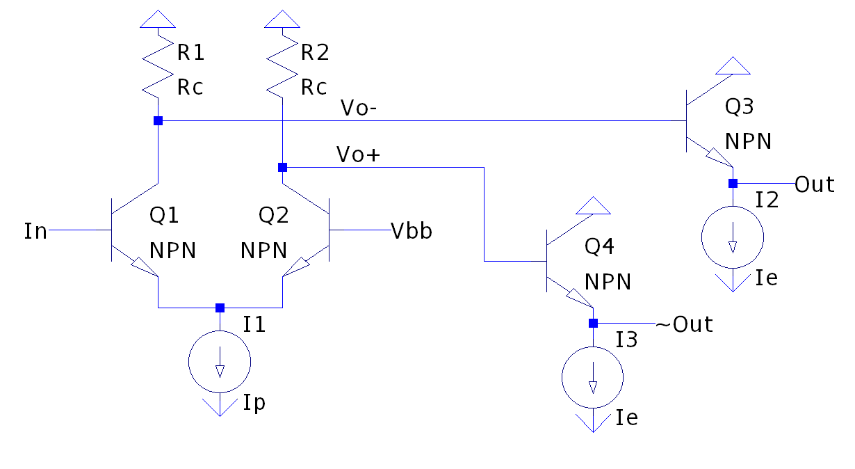
The first half of this circuit is a differential amplifier comparing the input to the gate and Vbb, which is a threshold voltage approximately in the center of the input voltage range. When $V_{in}$ is greater than $V_{bb}$, more current will flow through R1/Q1 and less current will flow through R2/Q2, so $V_o-$ will get more negative and $V_o+$ will get more positive. When $V_{in}$ is sufficiently high, essentially all of the current will flow through R1, producing a negative logic-low voltage on $V_o-$ and a zero logic-high voltage on $V_o+$.
The outputs use emitter follower buffers, which lets the output drive larger loads without affecting the operation of the differential pair. The emitter follower also shifts the logic levels down by one $V_{be}$, which leads to the funny logic levels associated with ECL.
One nice thing about ECL is most gates have a free inverting output (and inputs can often be inverted for free), which helps keep circuits fast. However, if this gate were to be used as an inverter, for example, the output buffer Q4 could be removed, as well as the resistor R2.
Choosing the voltage swing
The output voltage swing is affected by the current through the gate and the value of the collector resistors. Valid input levels will cause essentially all of the current to go through one side of the differential pair, so the voltage on the side with current will be $-I_e R_c$ and the voltage on the other side will be almost zero. The output after the emitter follower will be (approximately) $-0.7V$ and $-0.7V-I_e R_c$. So to change the output swing, $I_e$ or $R_c$ must be changed.
The output swing affects the noise margins: larger output swings will have larger noise margins, both absolutely and relative to the total swing. A 1990 DEC research report on “Noise Issues in the ECL Circuit Family” discusses this in detail. Using their formulas, the noise margin for the 300mV swing I chose is about 60mV, which is low but hopefully not so low that it causes any spurious switching.
The output swing also affects the rise/fall times and therefore the speed of the gate, since most of the gate delay is in the rise/fall times. A larger swing is slower since it takes longer to charge the parasitic capacitances. This problem, like many, can be solved by throwing more power at it. Increasing the emitter current for all the transistors will help to speed up the gate, but the extra static power dissipation is not always worth it.
After choosing the voltage swing, the emitter current must be determined based on the desired speed. I put 3mA through the differential pairs and 1mA through the emitter follower level shifters, for a simulated maximum speed of about 85MHz. I was targeting 80MHz based on the maximum frequency of the function generators I have access to, knowing the real frequency would be slightly lower.
Getting rid of the current sources
What about that current source at the bottom? It can be replaced by a transistor current mirror (what happens in an integrated circuit situation), or by a simple resistor (what happens in a minimum-transistors situation like this).
Current mirrors can be pretty simple, and the bias generator can be shared among multiple gates, so it is only a single additional transistor per gate, but the transistor costs more than a resistor, both in parts and, more importantly, in board area, besides requiring an additional reference voltage to be routed between gates. So a resistor will have to do.
The problem with the resistor is the current won’t be constant anymore. As the input to the gate goes above $V_{bb}$, the voltage at the emitters of the transistors will also begin to rise above $V_{bb}-V_{be}$. As this voltage changes, the voltage across the resistor will increase and the current through the whole gate will increase. For a simple gate like the buffer shown above, this doesn’t affect operation much because when the input is high, all the current is going through the unused left leg of the circuit. However, if that leg is used, the output swing will be larger. The resistors used on the inverting outputs can be adjusted to account for this, but for multi-level topologies like the latch, the increased current affects both the true and complement outputs, so there isn’t really anything that can be done about it.
The effect of the increased current can be estimated without much trouble. When the input is below $V_{bb}$, the voltage at the top of the emitter resistor will be $V_{bb}-V_{be}$. This voltage is used to calculate the emitter resistor based on the desired current. When the input goes above Vbb, the voltage on the emitter resistor will be $V_{in}-V_{be}$, which will be about $V_{swing}/2$ higher than the value with a low input, since $V_{be}$ is pretty constant. The change in output voltage is then $(V_{swing}/2)*R_c/R_e$, which is 32mV for single level gates and 56mV for two-level gates. The change is larger for multi-level gates because the nominal voltage at the top of the emitter resistor is closer to the negative supply voltage, so the change in voltage because of the input represents a bigger percentage of the nominal voltage. Unfortunately, increasing the supply voltage to achieve better margins is an unattractive choice since the current must remain the same to achieve the same speed–the power dissipation goes up significantly. (I do plan to use a higher voltage to allow the use of gates with three levels. With a 3V supply, a three-level gate would end up with a nominal voltage of -2.9V at the bottom, which is way too close.)
Reference voltages
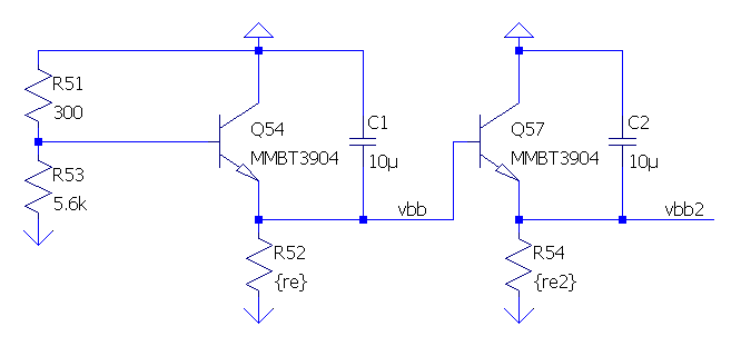
The $V_{bb}$ threshold voltage is placed in the center of the expected input levels. Since the input levels are $0V$ to $V_{swing}$ shifted down by the emitter followers, $V_{bb}$ is generated by shifting $V_{swing}/2$ using an identical emitter follower to match the output levels. The $V_{bb2}$ reference (for the inputs to multi-level gates) is generated in the same way.
Level shifting
Emitter followers are used for buffering and level shifting. The output voltage is the input voltage minus $V_{be}$, which is relatively constant since the current remains relatively constant (and more importantly, $V_{be}$ is exponentially related to the current, so a small change in current results in a tiny change in $V_{be}$). The standard output/input levels are generated from a single shift down, but multi-level gates require the levels to be shifted further down. This can be achieved by cascading emitter followers, or by stacking diode-connected transistors in the initial emitter follower. For reasons I am not entirely sure of, the stacked method resulted in decreased performance in my flip-flop.
Calculations summary
The collector resistors are easily calculated from the desired voltage swing and current.
$R_{c} = \frac {V_{swing}} {I_p} $ (100Ω)
The differential pair emitter resistors can be calculated from the voltage at the bottom of the gate and the supply voltage.
$ R_{ep} = \frac {V_{bb} - 0.7V + V_s} {I_p} $ (470Ω)
$ R_{ep2} = \frac {V_{bb2} - 0.7V + V_s} {I_p} $ (270Ω)
The emitter-follower resistors are calculated similarly:
$ R_e = \frac {V_s - (V_{swing}/2) - 0.7V} {I_e} $ (2.2kΩ)
$ R_e2 = \frac {V_s - (V_{swing}/2) - 1.4V} {I_e} $ (1.6kΩ)
The flip flop itself
A latch can be implemented as (D AND C) OR (Q AND NOT C). (See, for example
this 1983 Toshiba patent.
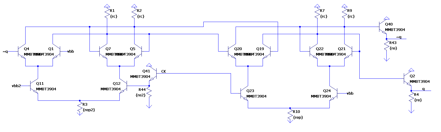
The latch forming the first part of this flip flop has the clock inverted. When CK is low, current takes the path through the left half of the latch. The output then takes on the value of the input. When CK is high, current takes the path through the right half of the latch, and the output is maintained at its present level. As the clock switches, there is a small glitch on the output as the current switches paths, but not enough to change directions. The clock input is shifted down to give room for the data input level above.
The second latch is the same topology as the first, but with the opposite clock polarity. It also uses the differential output of the first latch directly to save an emitter follower. This also means the clock can be used without the additional level shift. Finally, the emitter followers buffer the output.
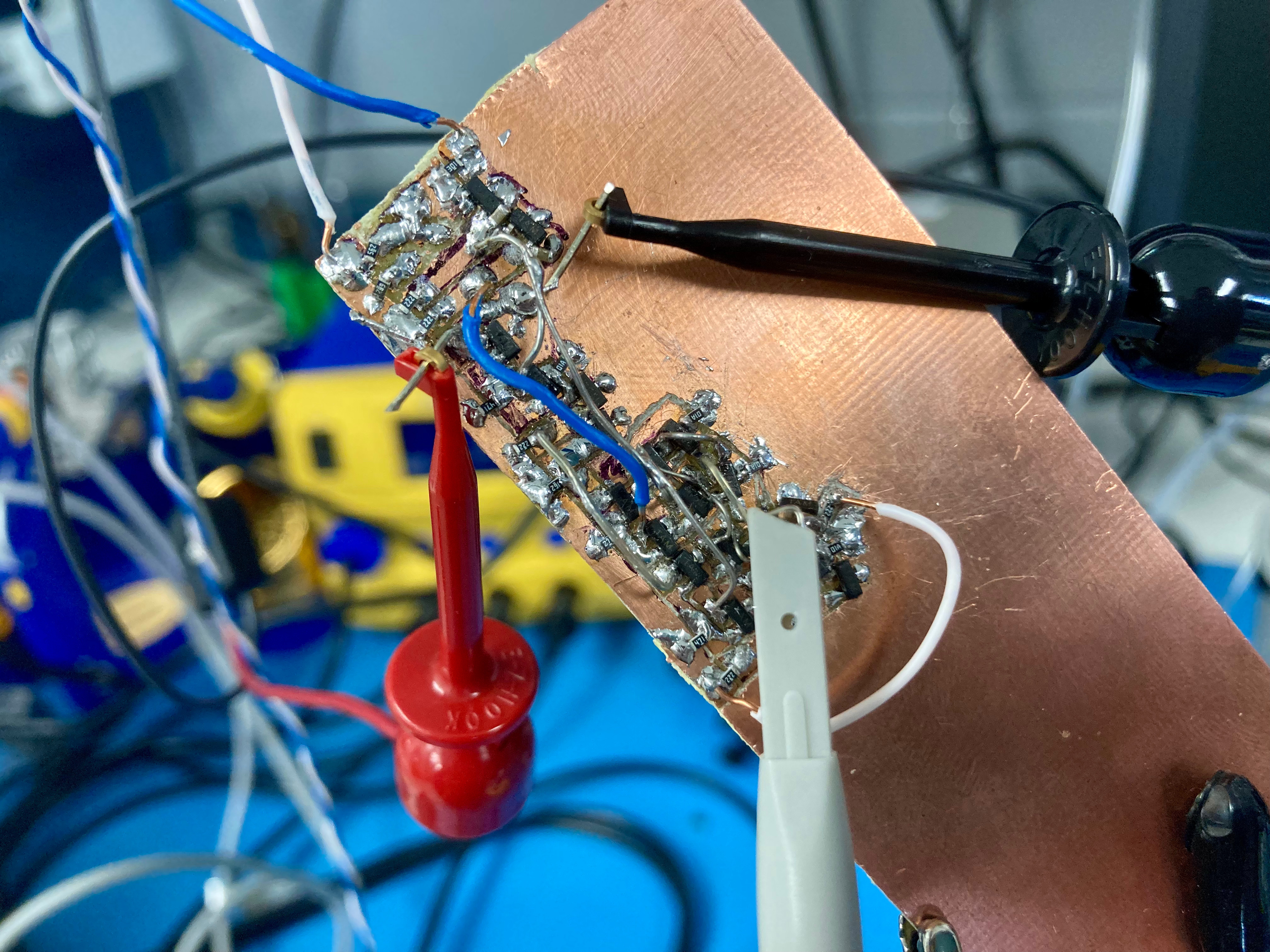
Building it!
Schematic, MMBT3904 symbol, and MMBT3904 model (from NXP)
The only changes from the previous revision are resistor values, so I used the same board and just replaced the resistors.
Pushing the limits
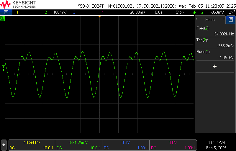
The frequency topped out at around 70MHz clock input. Since the function generator I was using only produces square waves up to 50MHz, I switched it to a sine wave with a larger (800mV) amplitude instead of the 300mV square wave. I initially was only able to hit 50MHz but I realized that it was due to the oscilloscope probes and their 11pF of additional capacitance. I stopped measuring the clock input, which gave me another 10MHz or so, and added a second emitter follower on the other output of the flip-flop to measure the output, which let me go all the way to 70MHz. This is slightly less than the simulation, probably because of the stray capacitance and other non-idealities that matter more at high frequency. (Actually, it is nearly the exact same percentage off as the simulation for the previous iteration. Perhaps something could be adjusted to achieve a more accurate simulation.) I ran into some problems with interference from broadcast FM, but they became less noticable after I stopped probing the clock lines.
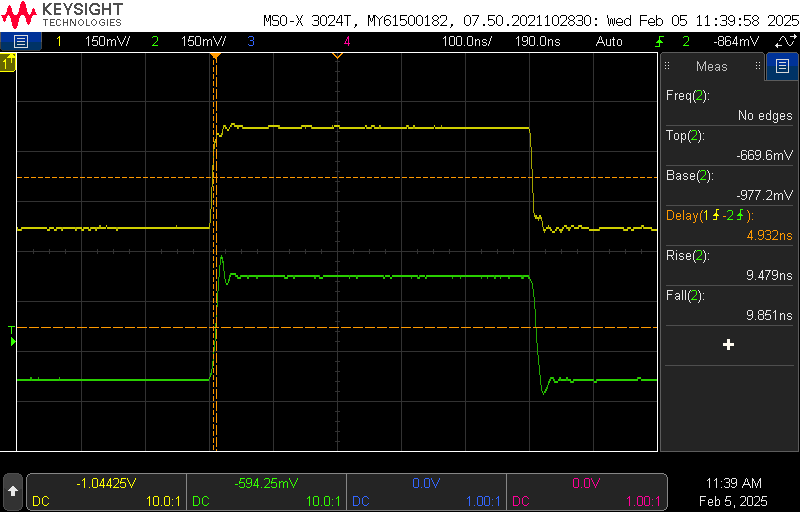
I again measured the clock buffer propagation delay. The results were pretty similar to the previous iteration, with a 10ns rise/fall time and a 5ns propagation delay. This time the flip flop was already connected, which likely impacted the speed. The simulation suggests 3-3.5ns delays, so the real-life conditions are a bit slower. I built a ring oscillator with the same parameters, which resulted in a 4.5ns delay per gate (with a 15pF probe in the loop).
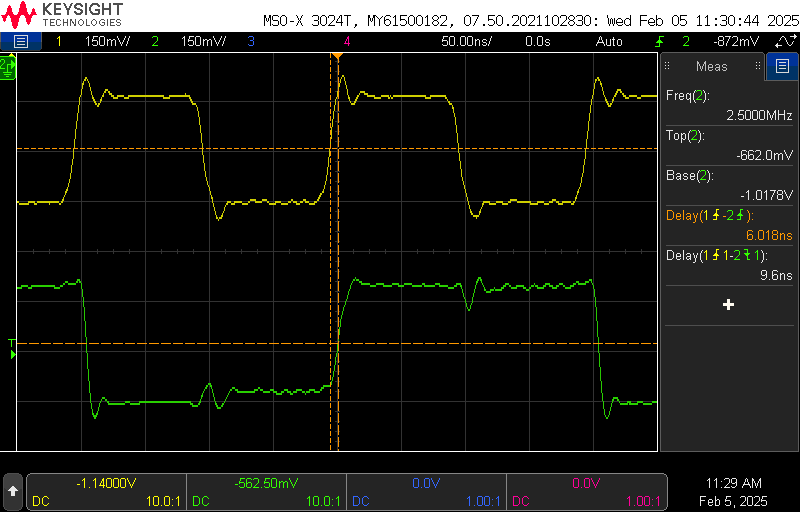
I measured a reduced clock-to-data delay of 6ns/10ns. This screenshot at 5MHz shows the effects of the resistor current source on the low edge as the clock changes, as well as the spikes associated with the negative clock edges.